

You're looking at a server memory listing that says something like DDR5-4800 CL40, DDR4-3200 CL16, or 16-18-18-38, and the smaller CL value appears to be the obvious winner. It isn't. CAS in RAM is a clock-cycle count, not a measurement in nanoseconds, so you need the memory data rate before you can judge first-word delay.
The practical fix is simple: calculate true CAS latency with latency(ns) = (CL × 2000) ÷ data rate(MT/s). Then check capacity, bandwidth, ECC, channel layout, NUMA placement, and stability before paying for tighter timings. On a virtualisation host or database server, those factors often matter more than reducing the first-word delay by a small amount.
Table of Contents
- What CAS in RAM Actually Means
- How CAS Latency Turns Into Real-World Delay
- Reading a Full Memory Timing String
- CAS Across DDR3, DDR4, and DDR5 Generations
- Why Memory Timing Matters for Hosted Workloads
- When Lower CL Numbers Do and Do Not Help
- Practical Guidance for Picking and Tuning RAM
What CAS in RAM Actually Means
A developer or sysadmin usually meets CAS while decoding a DIMM label, BIOS screen, or procurement spreadsheet. A line such as DDR4-3200 CL16 contains two different ideas: the module's transfer rate and the number of memory clock cycles the controller waits before the first requested data appears.
CAS means Column Address Strobe. DRAM organises storage into rows and columns. The memory controller first activates a row with the Row Address Strobe, or RAS, and then selects a column within that open row. CAS latency, written as CL, counts the clock cycles between the read command and the arrival of the first valid data from the module. The CAS latency reference describes this as the interval between a read command and data availability.
That sequence matters because the first CL number doesn't describe the speed of the memory bus. A module with CL40 can transfer data across a faster interface than a CL16 module, while a CL16 module can still have a longer delay in nanoseconds if its clock is slower.
Practical rule: Never compare CL values without comparing the associated data rates.
CAS primarily describes the read path. Writes use related timings, including write command to data timing, and a complete memory access also depends on row activation, precharge, refresh, and controller scheduling. The first number is useful, but it isn't a complete performance profile.
A timing label such as 16-18-18-38 begins with CL16, but the remaining values describe other parts of the DRAM command sequence. That broader timing string becomes important when a system is unstable, when a BIOS chooses conservative defaults, or when mixed DIMMs force the platform to train memory at a slower setting.
For a server operator, the useful translation is this: CAS tells you how long the controller waits in cycles for the first word after a suitable read command. It doesn't tell you whether the host has enough RAM, whether all memory channels are populated, or whether a virtual machine is remote from the NUMA node holding its pages.
How CAS Latency Turns Into Real-World Delay
A hosted database misses its target latency, and the memory specification shows CL40 instead of the familiar CL16. That label alone does not explain the delay. Convert the cycle count and data rate into nanoseconds first:
latency(ns) = (CL x 2000) / data rate(MT/s)
The factor of 2000 accounts for double data rate transfers. The result estimates the first-word CAS delay, not the complete time for every DRAM access. Row misses, request queueing, controller policy, and other timings can increase observed latency.
Work through the calculation
For DDR4-3200 CL16:
(16 x 2000) / 3200 = 10.0 ns
For DDR5-6000 CL30:
(30 x 2000) / 6000 = 10.0 ns
DDR5 has nearly twice the CL number, yet its faster transfer rate produces the same approximate CAS delay. A memory manufacturer's speed and latency guide uses the same relationship, showing DDR5-4800 CL40 at about 16.7 ns and DDR5-5600 CL46 at about 16.4 ns.
The examples also show why raw CL can mislead. DDR3-1866 CL9 is about 9.64 ns, DDR3-2133 CL12 about 11.25 ns, and DDR4-2666 CL13 about 9.75 ns. A lower cycle count does not automatically mean less time.
| Kit | CL Cycles | Data Rate (MT/s) | Latency (ns) |
|---|---|---|---|
| DDR4-3200 CL16 | 16 | 3200 | 10.0 |
| DDR4-3600 CL9 | 9 | 3600 | 5.0 |
| DDR5-6000 CL30 | 30 | 6000 | 10.0 |
| DDR5-4800 CL40 | 40 | 4800 | 16.7 |
| DDR5-5600 CL46 | 46 | 5600 | 16.4 |
The calculation describes first-word delay. It does not remove bandwidth differences. Higher data rates move more data per unit of time, so a DDR5 host can provide substantially more throughput even when its calculated CAS delay matches DDR4.
That distinction matters in hosted workloads. A cache lookup or pointer-heavy structure may wait on the first word. A backup stream, compression pipeline, or analytics scan may spend more time consuming sustained bandwidth. Capacity, channel configuration, and stable operation can matter more than a small CAS improvement when the workload is memory-heavy.
Reading a Full Memory Timing String
A timing string such as 16-18-18-38 is a compact description of several delays. The first value is tCL, or CAS latency. The second is tRCD, the delay between activating a row and accessing a column. The third is tRP, the time required to precharge or close the current row before activating another. The fourth is tRAS, the minimum time a row must remain active.
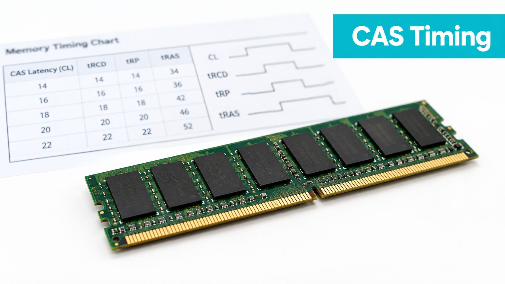
A row hit can avoid some activation work because the needed row is already open. A row miss may require precharge, activation, and column access before the controller can return data. That's why a module's practical access behaviour can't be inferred from tCL alone.
What the four primary values control
| Position | Timing | Meaning |
|---|---|---|
| First | tCL | Cycles from the read command to first data |
| Second | tRCD | Delay from row activation to column access |
| Third | tRP | Time to close one row before opening another |
| Fourth | tRAS | Minimum active time for an opened row |
The timing string may hide important secondary and tertiary values. tRFC controls refresh-related timing, tWR governs write recovery, and tRRD affects delays between row activations. Firmware often applies these automatically through memory training, while advanced BIOS menus expose more controls for manual tuning.
A lower value isn't universally safer or faster. Each timing has electrical and platform constraints, and reducing one value can require a lower data rate, higher voltage, or additional validation. Registered ECC DIMMs, unbuffered ECC DIMMs, and consumer modules also follow different platform rules, so a value copied from one class of hardware may be unsuitable for another.
The BIOS usually presents the primary timings first because they're easy to understand and useful for compatibility checks. Advanced controls can alter refresh behaviour, rank timing, command rate, and other interactions that become important under sustained load.
CAS dominates casual discussion because it appears first and often looks like the most prominent number. In reality, a DRAM access is governed by a much larger timing set. Treat CL as an entry point into the timing model, not as a complete verdict on module performance.
CAS Across DDR3, DDR4, and DDR5 Generations
A server upgrade can show a higher CL number while delivering similar first-word latency. That happens because newer memory transfers data faster, so each clock cycle is shorter. Comparing CL alone is like comparing the number of steps in two staircases without checking the height of each step.
The historical examples make the calculation concrete. DDR3-1866 CL9 works out to about 9.64 ns, DDR3-2133 CL12 to about 11.25 ns, and DDR4-2666 CL13 to about 9.75 ns. The DRAM technology teaching material shows how earlier DRAM described timing differently, including a typical 60 ns access-time example with a CAS access time around 15 ns and a CAS latency of 3.
The table applies the supplied conversion formula to example modules. These figures illustrate first-word timing, not application performance.
| Generation | Example Module | CAS Latency (CL) | Clock Speed (MT/s) | True Latency (ns) | Typical Use |
|---|---|---|---|---|---|
| DDR3 | DDR3-1600 CL11 | 11 | 1600 | 13.75 | Older servers and desktops |
| DDR4 | DDR4-3200 CL16 | 16 | 3200 | 10.0 | Current general-purpose servers and desktops |
| DDR5 | DDR5-6400 CL32 | 32 | 6400 | 10.0 | Newer high-bandwidth platforms |
DDR5 often has a higher CL count than DDR4 because its transfer rate is higher. One industry explanation places common DDR5 modules in the CL30 to CL40 range and describes real latency around 9 to 14 ns, while also highlighting the generation's higher bandwidth. The calculation above shows why a larger CL number does not automatically mean slower absolute response.
DDR5 also changes how the platform moves data. Its longer burst behaviour and split-channel organisation influence memory-controller scheduling and the value of parallel access. CPU memory-controller design, DIMM population, rank layout, firmware, and workload access patterns can outweigh a small CAS difference.
For hosted systems, the comparison is practical rather than cosmetic. A memory-intensive virtualisation node may gain more from bandwidth and sufficient capacity than from a tighter CL. A pointer-heavy service may benefit from lower true latency, but only if CPU scheduling, storage, NUMA placement, and memory pressure are already under control.
ECC server RDIMMs add further constraints. Registered buffering, error correction, supported density, and vendor qualification can matter more than the lowest available CL. Samsung, SK Hynix, and Micron modules may expose different JEDEC profiles, so validate the DIMM against the CPU and board documentation instead of choosing by label alone.
For EPYC systems, check channel and DIMM population guidance before tuning timings. A dedicated AMD EPYC server helps only when its memory topology fits the workload and operating model. CL without transfer rate, capacity, and platform context is an incomplete specification.
Why Memory Timing Matters for Hosted Workloads
A hosted node rarely runs one isolated benchmark. It runs virtual machines, databases, application workers, caches, backup processes, monitoring agents, and host services at the same time. That changes the buying question from "Which DIMM has the lowest CL?" to "Which memory configuration keeps the whole node responsive under contention?"
Latency can matter in pointer-heavy paths. Redis and Memcached issue frequent lookups, PostgreSQL and MySQL InnoDB depend on buffer-pool access, and JVM or .NET heaps can create irregular access patterns during allocation and garbage collection. These workloads may benefit from lower true latency when the CPU repeatedly waits for data that isn't already in a cache.
That benefit isn't automatic. A database with insufficient memory may page or evict useful data, making additional capacity more valuable than a tighter CAS setting. A virtual machine can also suffer from CPU scheduling, storage latency, noisy neighbours, or remote NUMA access before DRAM timing becomes the dominant delay.
Where the platform changes the result
Dual-socket servers divide memory into NUMA nodes. A process accessing memory attached to the other socket can encounter a different path from a process using local memory. KVM and VMware can schedule virtual CPUs and memory across those nodes, while pinning and placement policies influence locality. A faster DIMM cannot fully compensate for poor NUMA placement.
Rank interleaving and channel population affect throughput as well. A host with balanced channels and suitable rank diversity can keep more memory paths active. That may produce a larger practical improvement for a bandwidth-bound tenant mix than moving between modules with similar nanosecond CAS latency.
Production observation: On multi-tenant infrastructure, operators usually notice memory pressure, swap activity, NUMA imbalance, or sustained bandwidth saturation before they can isolate a small CAS difference. Stable capacity and predictable topology make better operational improvements than chasing the lowest label.
Workload categories respond differently:
- In-memory caches: First-word delay can matter when requests perform many random lookups.
- OLTP databases: Timing can help some read-heavy, latency-sensitive queries, but capacity and buffer-pool residency usually come first.
- Virtual machine hosts: Channel balance, NUMA locality, ECC behaviour, and density often outweigh small CL changes.
- Backups and object storage: Sustained bandwidth, storage throughput, network capacity, and queueing dominate many transfers.
- Network-bound APIs: Application and network delays can hide modest DRAM timing differences.
The practical hierarchy is capacity, stability, topology, bandwidth, then CAS tuning, unless measurement proves a particular workload is stalled on memory latency. High-memory deployments should be evaluated as a complete system, including DIMM density and NUMA layout. A high-memory dedicated hosting configuration can be a better answer than a smaller node with tighter timings when the workload's working set exceeds available RAM.
When Lower CL Numbers Do and Do Not Help
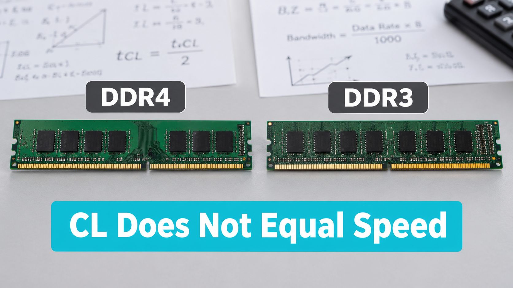
A server administrator comparing two DIMMs may see a smaller CL value and assume it will respond faster. That conclusion works only when the modules use the same data rate and operate under compatible platform conditions. Convert the timing to nanoseconds before comparing them.
Applying the conversion formula from the earlier section, the CL11 DDR3 module reaches 13.75 ns, while the DDR4 and DDR5 examples both reach 10.0 ns. The smaller label is not automatically the shorter delay. A memory timing primer from a major module vendor makes the same broader point: identical CL values can represent different real delays at different memory speeds.
Workloads that can expose timing
Lower true latency matters most when the processor performs repeated random reads and has little opportunity to hide memory delay. A small latency-sensitive cache, a single-threaded query path, or a pointer-heavy service can fit this pattern when frequent working-set misses reach DRAM instead of the CPU cache.
A hosted workload also needs a matching test method. sysbench memory can exercise memory operations, while STREAM measures sustained bandwidth. Database testing should use the actual engine and access pattern, such as a representative PostgreSQL or MySQL workload. A synthetic score alone cannot predict a service-level result.
Workloads that usually hide CAS
Streaming backups and compression jobs often depend more on sustained bandwidth, storage throughput, and network capacity. GPU pass-through jobs may spend most of their time in device memory. Network-bound APIs can be limited by application processing or the network path, while a capacity-limited host may spend more time handling page faults or swap activity than benefiting from a shorter first-word delay.
| Workload pattern | CAS priority | More important checks |
|---|---|---|
| Random in-memory lookups | Higher | True latency, CPU cache behaviour, contention |
| OLTP query execution | Moderate | Capacity, buffer pool, storage, NUMA locality |
| Streaming backup | Lower | Sustained bandwidth, storage, network path |
| Compression | Lower to moderate | CPU throughput, bandwidth, working-set size |
| Dense virtualisation | Moderate | Capacity, ECC, channels, NUMA placement |
| Network-bound API | Lower | Network and application latency |
Change one memory variable while holding the workload, CPU, storage, and scheduler configuration steady. If the service metric remains unchanged, CAS is not the useful tuning lever. If it improves, compare that gain with the added cost, power use, compatibility risk, and maintenance burden. For hosted systems, capacity, stable operation, topology, and bandwidth commonly deliver more practical value than the lowest CL label.
Practical Guidance for Picking and Tuning RAM
Start with compatibility, not CAS. Confirm whether the CPU and motherboard require ECC, registered DIMMs, or unbuffered modules, then check supported density, channel population, and qualified memory documentation. A module that looks faster on paper is useless if the platform downclocks it, refuses to train it, or becomes unreliable under sustained load.
Select a stable baseline
For servers and VPS nodes, a supported JEDEC profile is usually a stronger baseline than an exotic XMP or EXPO profile. Conservative settings can reduce compatibility surprises during long-running workloads, firmware changes, and thermal variation. The right choice depends on the platform, so record the actual speed and timings reported by firmware and the operating system rather than trusting the retail label.
Capacity comes before fine timing. If the host cannot keep active datasets in RAM, lower CAS won't fix paging or eviction pressure. The guidance in how much RAM a workload needs should be applied before comparing two otherwise compatible kits.
Validate one change at a time
- Record the baseline data rate, primary timings, voltage, DIMM population, NUMA layout, and workload result.
- Change one timing or one memory profile, not several settings at once.
- Run MemTest86 for a full validation cycle, then run a workload-shaped test such as
sysbench memoryorfio. - Check Linux EDAC records for corrected and uncorrected errors.
On Debian or Ubuntu systems, these commands provide useful verification:
sudo dmidecode --type memory
sudo lshw -class memory
sudo dmesg -T | grep -iE 'edac|ecc|memory'
sudo journalctl -k | grep -iE 'edac|ecc|mce'
For a memory throughput check with sysbench:
sysbench memory --memory-block-size=1M --memory-total-size=10G run
Use fio for storage tests rather than treating disk activity as a RAM benchmark:
fio --name=memory-adjacent-check --filename=/tmp/fio-test --size=1G --rw=read --bs=1M --direct=1 --runtime=60 --time_based --group_reporting
These commands don't prove that a timing change improved an application. They confirm what the platform configured and help expose errors or related bottlenecks.
Avoid silent downshifts
Mixed capacities, ranks, or module types can make firmware select the slowest common profile. Populate channels symmetrically where the platform manual requires it, and don't assume that adding a DIMM increases performance if it changes the operating mode. For a private cloud, document every node's memory population so migrations don't move a workload onto a materially different topology.
If a new setting fails, roll back to the saved BIOS profile or remove the changed DIMM set and reinstall the known-good configuration. Boot at the platform's default JEDEC settings, clear failed overclocking profiles, and rerun memory validation before making another adjustment. Keep a known-good spare kit available for swap testing, especially when diagnosing intermittent ECC or training failures.
The final decision should be evidence-based. Choose enough ECC memory, balanced channels, supported density, and reliable bandwidth first. Tune CAS only after measurements show that memory latency is limiting the service.
ARPHost, LLC provides VPS, bare metal servers, Proxmox private clouds, colocation, and managed infrastructure for teams that need stable memory capacity and predictable platform operation. If your workload needs more RAM, better NUMA planning, or a dedicated node for controlled tuning, visit ARPHost, LLC to discuss the right infrastructure.

Leave a Reply
You must be logged in to post a comment.